In this article we present a very simple model of a solar cell. Many notions presented in this chapter will be new but nonetheless the great lines of how a solar cell works should be clear. All the aspects presented in this chapter will be discussed in larger detail in the following chapters.
The working principle of solar cells is based on the photovoltaic effect, i.e. the generation of a potential difference at the junction of two different materials in response to electromagnetic radiation. The photovoltaic effect is closely related to the photoelectric effect, where electrons are emitted from a material that has absorbed light with a frequency above a material-dependent threshold frequency. In 1905, Albert Einstein understood that this effect can be explained by assuming that the light consists of well defined energy quanta, called photons. The energy of such a photon is given by
E = hν, (3.1)
where h is Planck’s constant and ν is the frequency of the light. For his explanation of the photoelectric effect Einstein received the Nobel Prize in Physics in 1921.
The photovoltaic effect can be divided into three basic processes:

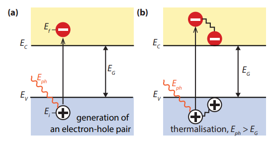
Figure 3.1: (a) Illustrating the absorption of a photon in a semiconductor with bandgap Eg. The photon with energy Eph = hν excites an electron from Ei to Ef. At Ei a hole is created. (b) If Eph > Eg, a part of the energy is thermalised.
1.Generation of charge carriers due to the absorption of photons in the materials that form a junction.
Absorption of a photon in a material means that its energy is used to excite an electron from an initial energy level Ei to a higher energy level Ef , as shown in Fig.1 (a). Photons can only be absorbed if electron energy levels Ei and Ef are present so that their difference equals to the photon energy, hν = Ef − Ei . In an ideal semiconductor electrons can populate energy levels below the so-called valence band edge, EV, and above the so called conduction band edge, EC. Between those two bands no allowed energy states exist, which could be populated by electrons. Hence, this energy difference is called the bandgap, Eg = EC − EV. If a photon with an energy smaller than Eg reaches an ideal semiconductor, it will not be absorbed but will traverse the material without interaction.
In a real semiconductor, the valence and conduction bands are not flat, but vary depending on the so-called k-vector that describes the crystal momentum of the semiconductor. If the maximum of the valence band and the minimum of the conduction band occur at the same k-vector, an electron can be excited from the valence to the conduction band without a change in the crystal momentum. Such a semiconductor is called a direct bandgap material. If the electron cannot be excited without changing the crystal momentum, we speak of an indirect bandgap material. The absorption coefficient in an direct bandgap material is much higher than in an indirect bandgap material, thus the absorber can be much thinner.
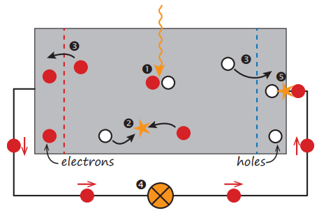
If an electron is excited from Ei to Ef , a void is created at Ei . This void behaves like a particle with a positive elementary charge and is called a hole. The absorption of a photon therefore leads to the creation of an electron-hole pair, as illustrated in Fig.2 Point 1. The radiative energy of the photon is converted to the chemical energy of the electron-hole pair. The maximal conversion efficiency from radiative energy to chemical energy is limited by thermodynamics. This thermodynamic limit lies in between 67% for non-concentrated sunlight and 86% for fully concentrated sunlight.
2.Subsequent separation of the photo-generated charge carriers in the junction.
Usually, the electron-hole pair will recombine, i.e. the electron will fall back to the initial energy level Ei , as illustrated in Fig.2 Point 2. The energy will then be released either as photon (radiative recombination) or transferred to other electrons or holes or lattice vibrations (nonradiative recombination). If one wants to use the energy stored in the electron-hole pair for performing work in an external circuit, semipermeable membranes must be present on both sides of the absorber, such that electrons only can flow out through one membrane and holes only can flow out through the other membrane, as illustrated in Fig. 2 Point 3. In most solar cells, these membranes are formed by n- and p-type materials.

Figure 2: A very simple solar cell model. Point 1 Absorption of a photon leads to the generation of an electron-hole pair. Point 2 Usually, the electrons and holes will combine. Point 3 With semipermeable membranes the electrons and the holes can be separated. Point 4 The separated electrons can be used to drive an electric circuit. Point 5 After the electrons passed through the circuit, they will recombine with holes.
A solar cell has to be designed such that the electrons and holes can reach the membranes before they recombine, i.e. the time it requires the charge carriers to reach the membranes must be shorter than their lifetime. This requirement limits the thickness of the absorber.
3. Collection of the photo-generated charge carriers at the terminals of the junction.
Finally, the charge carriers are extracted from the solar cells with electrical contacts so that they can perform work in an external circuit (Fig.2 Point 4). The chemical energy of the electron-hole pairs is finally converted to electric energy. After the electrons passed through the circuit, they will recombine with holes at a metalabsorber interface, as illustrated in Fig.2 Point 5.
4.Loss mechanisms
The two most important loss mechanisms in single bandgap solar cells are the inability to convert photons with energies below the bandgap to electricity and thermalisation of photon energies exceeding the bandgap, as illustrated in Fig. 1 (b). These two mechanisms alone amount to the loss of about half the incident solar energy in the conversion process. Thus, the maximal energy conversion efficiency of a singlejunction solar cell is considerably below the thermodynamic limit. This single bandgap limit was first calculated by Shockley and Queisser in 1961.
